- 您现在的位置:买卖IC网 > Sheet目录381 > 4257-00 (Peregrine Semiconductor)KIT EVAL FOR 4257 RF SWITCH
�� �
�
�PE4257�
�Product� Specification�
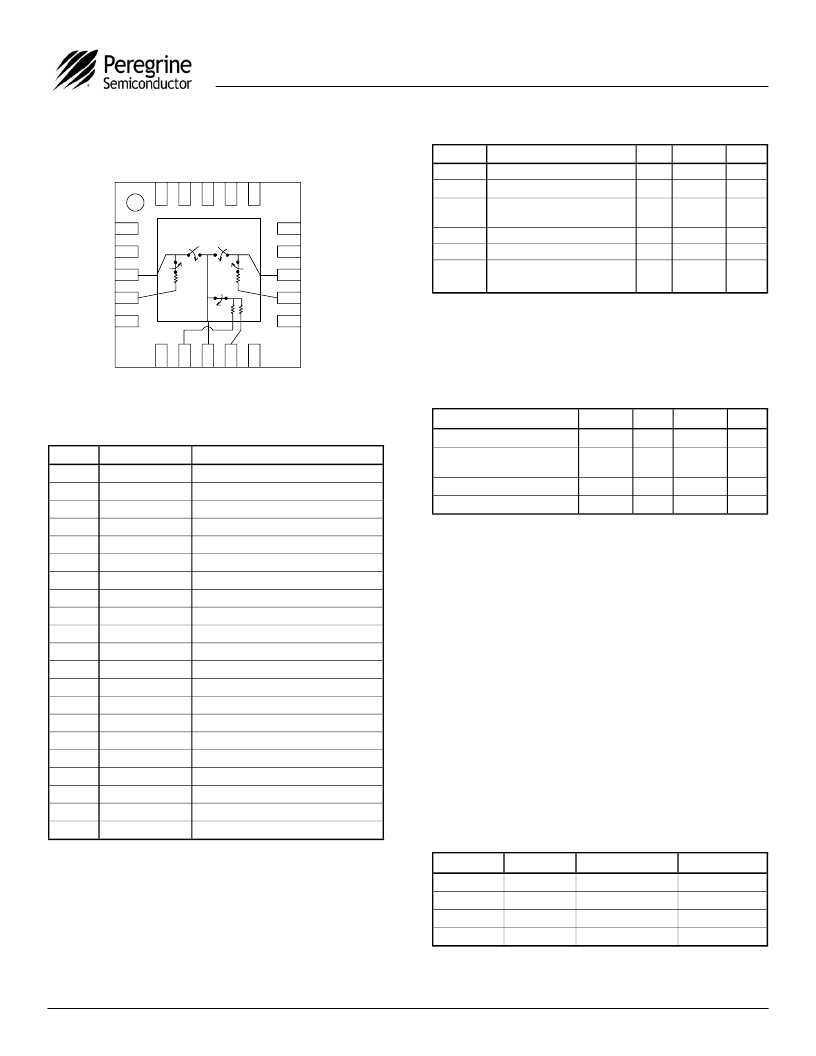
�Figure� 3.� Pin� Configuration� (Top� View)�
�Table� 3.� Absolute� Maximum� Ratings�
�Symbol�
�V� DD�
�V� I�
�Parameter/Condition�
�Power� supply� voltage�
�Voltage� on� any� DC� input�
�Min�
�-0.3�
�-0.3�
�Max�
�4.0�
�V� DD� +� 0.3�
�Units�
�V�
�V�
�GND�
�GND�
�RF1�
�1�
�2�
�3�
�GND�
�15� GND�
�14� GND�
�13�
�RF2�
�P� RF�
�T� ST�
�T� OP�
�V� ESD�
�RF� power� on� RFC,� RF1,� RF2�
�On� Port/� Terminated� Port�
�Storage� temperature�
�Operating� temperature�
�ESD� voltage�
�(Human� Body� Model)�
�-65�
�-40�
�1000�
�33/24�
�+150�
�+85�
�dBm�
�°C�
�°C�
�V�
�GND,� RF1� Term.�
�GND�
�4�
�5�
�12� GND,� RF2� Term.�
�11� GND�
�Exceeding� absolute� maximum� ratings� may� cause�
�permanent� damage.� Operation� should� be� restricted� to�
�the� limits� in� the� Operating� Ranges� table.� Operation�
�between� operating� range� maximum� and� absolute�
�maximum� for� extended� periods� may� reduce� reliability.�
�4x4mm� 20-Lead� QFN�
�Table� 4.� Operating� Ranges� @� 25� °C�
�Parameter�
�Min�
�Typ�
�Max�
�Unit�
�Table� 2.� Pin� Descriptions�
�V� DD� Power� Supply�
�2.7�
�3.0�
�3.3�
�V�
�No.�
�1�
�2�
�3� 1�
�Name�
�GND�
�GND�
�RF1�
�RF� Ground�
�RF� Ground�
�RF� I/O�
�Description�
�I� DD� Power� Supply� Current�
�(V� DD� =� 3V,� V� CNTL� =� 3V)�
�Control� Voltage� High�
�Control� Voltage� Low�
�0.70� V� DD�
�0�
�8�
�20�
�0.30� V� DD�
�μ� A�
�V�
�V�
�4�
�5�
�6�
�7�
�8� 1�
�9�
�10�
�11�
�12�
�13� 1�
�14�
�15�
�16� 2�
�17� 2�
�18� 3�
�19�
�20�
�GND�
�GND�
�GND�
�GND�
�RFC�
�GND�
�GND�
�GND�
�GND�
�RF2�
�GND�
�GND�
�CTRL2�
�CTRL1�
�VSS� /� GND�
�GND�
�VDD�
�RF� Ground�
�RF� Ground�
�RF� Ground�
�RF� Ground�
�RF� Common�
�RF� Ground�
�RF� Ground�
�RF� Ground�
�RF� Ground�
�RF� I/O�
�RF� Ground�
�RF� Ground�
�Control� 2�
�Control� 1�
�Negative� Supply� Option�
�Digital� Ground�
�Supply�
�Latch-Up� Avoidance�
�Unlike� conventional� CMOS� devices,� UltraCMOS?�
�devices� are� immune� to� latch-up.�
�Electrostatic� Discharge� (ESD)� Precautions�
�When� handling� this� UltraCMOS?� device,� observe� the�
�same� precautions� that� you� would� use� with� other� ESD-�
�sensitive� devices.� Although� this� device� contains�
�circuitry� to� protect� it� from� damage� due� to� ESD,�
�precautions� should� be� taken� to� avoid� exceeding� the�
�rating� specified.�
�Switching� Frequency�
�The� PE4257� has� a� maximum� 25� kHz� switching� rate�
�when� the� internal� negative� voltage� generator� is� used�
�(pin� 18=GND).� The� rate� at� which� the� PE4257� can� be�
�switched� is� only� limited� to� the� switching� time� if� an�
�external� -3� V� supply� is� provided� at� (pin18=V� SS� ).�
�Pad� GND� RF� Ground� Pad�
�Notes:� 1.� RF� pins� 3,� 8,� and� 13� must� be� at� 0� VDC.� The� RF� pins� do�
�not� require� DC� blocking� capacitors� for� proper� operation� if� the�
�Table� 5.� Truth� Table�
�CTRL1� CTRL2�
�RFC� –� RF1�
�RFC� –� RF2�
�0� VDC� requirement� is� met.�
�2.� Pins� 16� and� 17� are� the� CMOS� controls� that� set� the� four�
�operating� states.�
�3.� Connect� pin� 18� to� GND� to� enable� the� negative� voltage�
�generator.� Connect� pin� 18� to� V� SS� (-3� V)� to� bypass� and�
�Low�
�Low�
�High�
�High�
�Low�
�High�
�Low�
�High�
�OFF�
�OFF�
�ON�
�N/A� 1�
�OFF�
�ON�
�OFF�
�N/A� 1�
�disable� internal� -3� V� supply� generator.� See� paragraph�
�“Switching� Frequency.”�
�?2004-2009� Peregrine� Semiconductor� Corp.� All� rights� reserved.�
�Notes:� 1.� The� operation� of� the� PE4257� is� not� supported� or�
�characterized� in� the� C1=V� DD� and� C2=V� DD� state.�
�Document� No.� 70-0166-06� │� UltraCMOS?� RFIC� Solutions�
�Page� 2� of� 7�
�Logo� updated� under� non-rev� change.� Peregrine� products� are� protected� under� one� or� more� of� the� following� U.S.� Patents:� http://patents.psemi.com�
�发布紧急采购,3分钟左右您将得到回复。
相关PDF资料
426013700-3
CABLE EXT PWR IN 4WIRE LEADS
426090200-3
CABLE SERIAL IN RS-232 CONN
426120410-3
CABLE OSD 12-WAY 610MM
4268-00
KIT EVAL FOR 4268 RF SWITCH
4270-00
KIT EVAL FOR 4270 RF SWITCH
4271-00
KIT EVAL FOR 4271 RF SWITCH
4272-00
KIT EVAL FOR 4272 RF SWITCH
4273-00
KIT EVAL FOR 4273 RF SWITCH
相关代理商/技术参数
4257-01
制造商:PEREGRINE 制造商全称:PEREGRINE 功能描述:50 ?SPDT Absorptive UltraCMOS? DC ? 3.0 GHz RF Switch
425701-000
制造商:TE Connectivity 功能描述:Conn Wire to Board SKT 40 POS 1.27mm ST Cable Mount 制造商:TE Connectivity 功能描述:425701-000 - Bulk
4257-02
制造商:PEREGRINE 制造商全称:PEREGRINE 功能描述:50 ?SPDT Absorptive UltraCMOS? DC ? 3.0 GHz RF Switch
42570-NISTL
制造商:EXTECH-FLIR COMMERCIAL SYSTEMS 功能描述:IR THERMOMETER WITH LIMITED NIST, 42570
4257-12JL
制造商:Rochester Electronics LLC 功能描述:- Bulk
42571540
制造商: 功能描述: 制造商:undefined 功能描述:
42573K
制造商:Integrated Device Technology Inc 功能描述:
42573K WAF
制造商:Integrated Device Technology Inc 功能描述: